
-
COMPANY
-
BUSINESS
-
CSR
-
CAREERS
-
MEDIA
-
CONTACT
-
COMPANY
-
BUSINESS
-
CSR
-
CAREERS
-
MEDIA
-
CONTACT
 ☰
☰
☰
☰

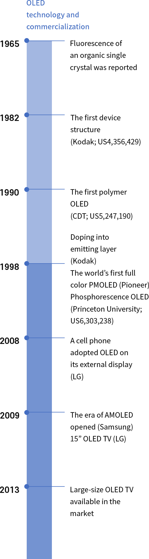
Challenges make changes
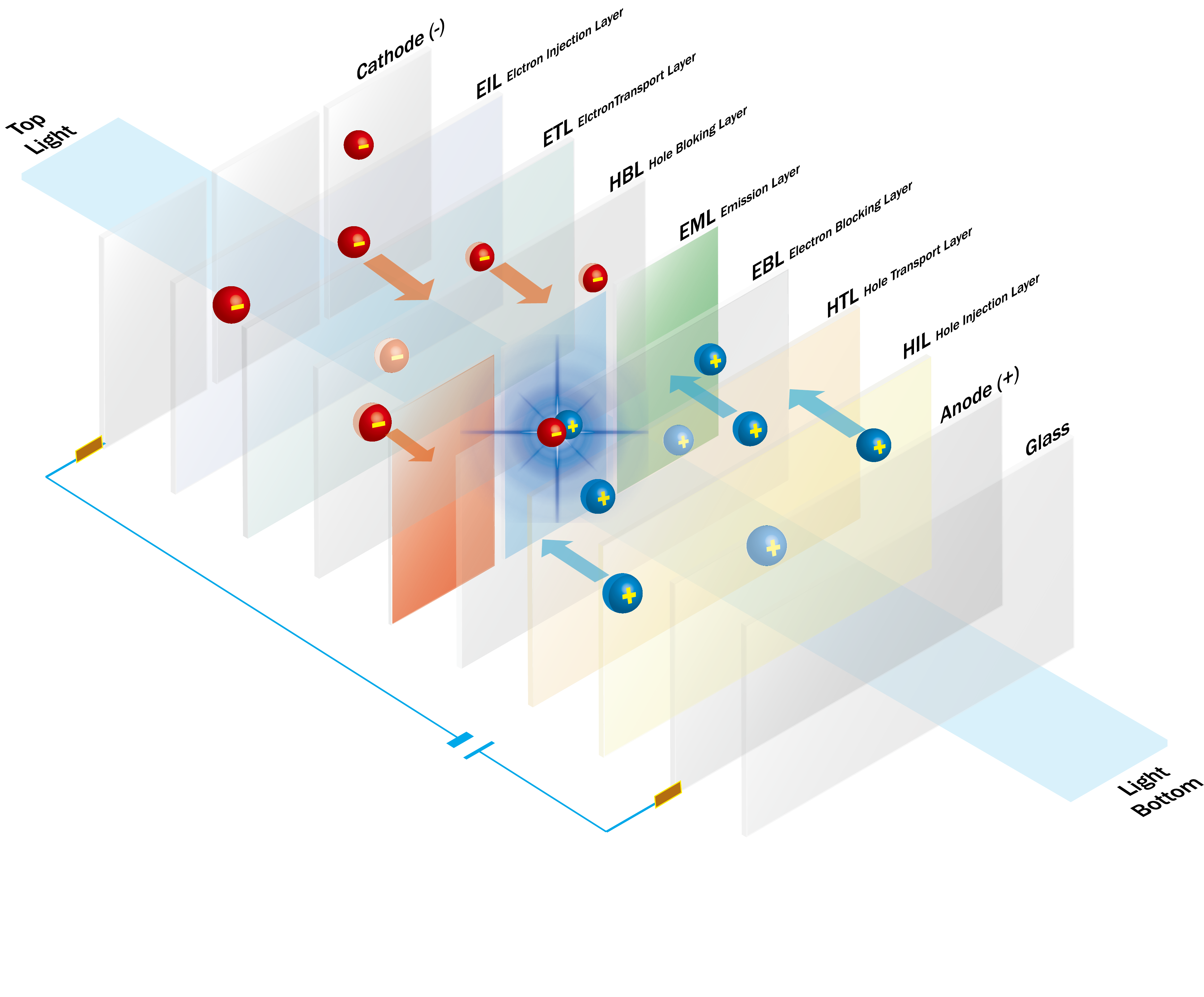
 OLED uses the phenomenon in which holes (positively charged) injected from anode (+) and negatively charged electrons from cathode (-) recombine in the emitting layer to form excitons which emit light while returning to the ground energy state.
Several organic materials including hole injection layer (HIL), hole transport layer (HTL), electron injection layer (EIL), and electron transport layer (ETL) are added between the electrodes in a specified thickness for more effective recombination of holes and electrons in the emitting layer. More and more sophisticated device structures and materials are being proposed, for example, doping, and multi-layered HTL and ETL.
In addition, many efforts have been made to maximize the device performance by optimizing various parameters such as charge balance, transporting speed, recombination location and contours. To maximize the efficiency and lifetime, diverse device structures were developed such as tandem structure which connects two or more OLED units with charge generation layer (CGL) acting as an electrode connecting the units. Organic materials for OLED may be classified into fluorescent and phosphorescent materials according to their emitting mechanisms. They include emitting layers of 3 primary colors of red, green and blue, hole injection layer, hole transport layer, electron injection layer, electron transport layer and capping layer which may be additionally configured on top of OLED device’s electrode to maximize light extraction and improve viewing angle.
Fluorescent materials emit light when excitons at its excited S1 state return to the ground state S0. The efficiency limit is 25% (=1/4), the ratio of physically generated singlet. Meanwhile, phosphorescent materials leverage the spin-orbit coupling effect of heavy metals such as Iridium (Ir) and Platinum (Pt) to additionally harness triplet excitons of 75% (=3/4), which, therefore, theoretically can show 100% efficiency. Recently, the commercial potential of thermally activated delayed fluorescence (TADF) materials is getting attention as they can achieve 100% efficiency using the reverse inter-system crossing (RISC) phenomenon which can be observed when a material has a very small difference in energy levels between S1 and T1. However, TADF materials retain a broad of spectrum resulting in lower color purity. Also, because the required T1 level for the blue host should be too high, it raises the challenges of prolonging lifetime with lots of limitations on molecular design. In order to resolve the inherent issues of originally-proposed TADF, hyperfluorescence devices partly supported by the advantages of fluorescent dopant with a narrower spectrum and longer lifetime are actively being developed.
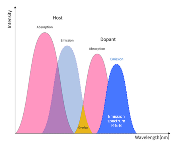
Phosphorescent materials have long been adopted in red and green emitting layers, and fluorescent materials are being employed only on blue emitting layers. Each emitting layer is comprised of host(s) and dopant(s). In the emitting layer, energy transfer mechanism involves an overlap of host’s emission spectrum and dopant’s absorption spectrum so that the dopant releases the energy absorbed in the form of an electroluminescent spectrum. Numerous theoretical and experimental approaches are known for optimizing molecular structures, and physical and electrical properties to transfer the energy from host to dopant more effectively while minimizing the losses.
OLED uses the phenomenon in which holes (positively charged) injected from anode (+) and negatively charged electrons from cathode (-) recombine in the emitting layer to form excitons which emit light while returning to the ground energy state.
Several organic materials including hole injection layer (HIL), hole transport layer (HTL), electron injection layer (EIL), and electron transport layer (ETL) are added between the electrodes in a specified thickness for more effective recombination of holes and electrons in the emitting layer. More and more sophisticated device structures and materials are being proposed, for example, doping, and multi-layered HTL and ETL.
In addition, many efforts have been made to maximize the device performance by optimizing various parameters such as charge balance, transporting speed, recombination location and contours. To maximize the efficiency and lifetime, diverse device structures were developed such as tandem structure which connects two or more OLED units with charge generation layer (CGL) acting as an electrode connecting the units. Organic materials for OLED may be classified into fluorescent and phosphorescent materials according to their emitting mechanisms. They include emitting layers of 3 primary colors of red, green and blue, hole injection layer, hole transport layer, electron injection layer, electron transport layer and capping layer which may be additionally configured on top of OLED device’s electrode to maximize light extraction and improve viewing angle.
Fluorescent materials emit light when excitons at its excited S1 state return to the ground state S0. The efficiency limit is 25% (=1/4), the ratio of physically generated singlet. Meanwhile, phosphorescent materials leverage the spin-orbit coupling effect of heavy metals such as Iridium (Ir) and Platinum (Pt) to additionally harness triplet excitons of 75% (=3/4), which, therefore, theoretically can show 100% efficiency. Recently, the commercial potential of thermally activated delayed fluorescence (TADF) materials is getting attention as they can achieve 100% efficiency using the reverse inter-system crossing (RISC) phenomenon which can be observed when a material has a very small difference in energy levels between S1 and T1. However, TADF materials retain a broad of spectrum resulting in lower color purity. Also, because the required T1 level for the blue host should be too high, it raises the challenges of prolonging lifetime with lots of limitations on molecular design. In order to resolve the inherent issues of originally-proposed TADF, hyperfluorescence devices partly supported by the advantages of fluorescent dopant with a narrower spectrum and longer lifetime are actively being developed.
Phosphorescent materials have long been adopted in red and green emitting layers, and fluorescent materials are being employed only on blue emitting layers. Each emitting layer is comprised of host(s) and dopant(s). In the emitting layer, energy transfer mechanism involves an overlap of host’s emission spectrum and dopant’s absorption spectrum so that the dopant releases the energy absorbed in the form of an electroluminescent spectrum. Numerous theoretical and experimental approaches are known for optimizing molecular structures, and physical and electrical properties to transfer the energy from host to dopant more effectively while minimizing the losses.